 Boards
This is a gallery of the circuit boards I've made for the Megaprocessor.
Logic Functions:
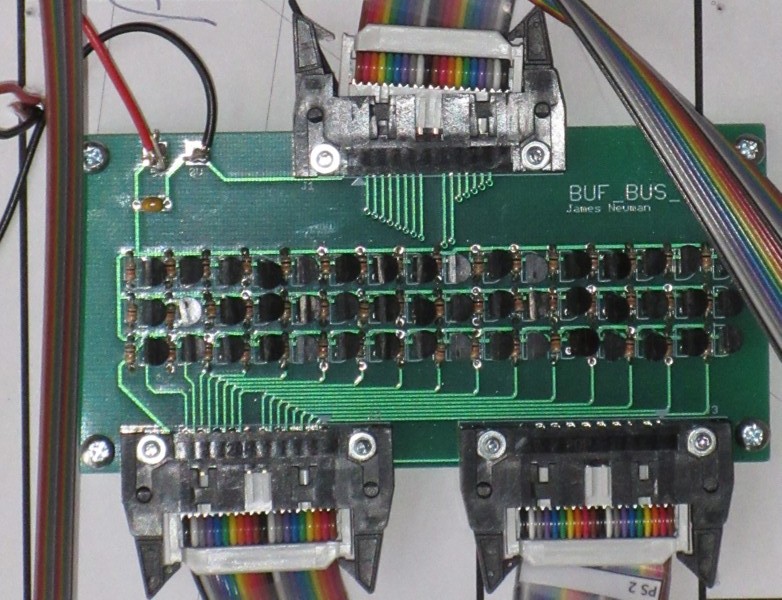
| 1 BUF (design files) |
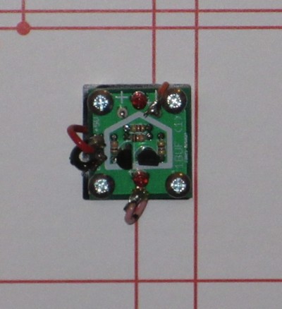 |
| 2 AND (design files) |
 |
| 2 OR (design files) |
 |
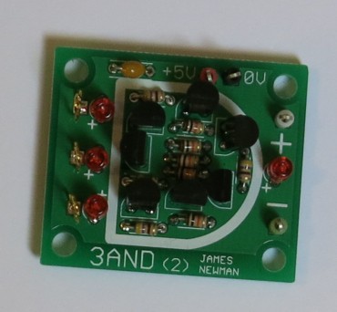
| 3 AND (design files) |
 |
| 3 OR (design files) |
 |
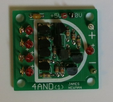
| 4 AND (design files) |
 |
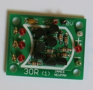
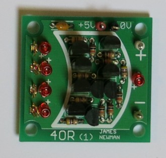
| 4 OR (design files) |
 |
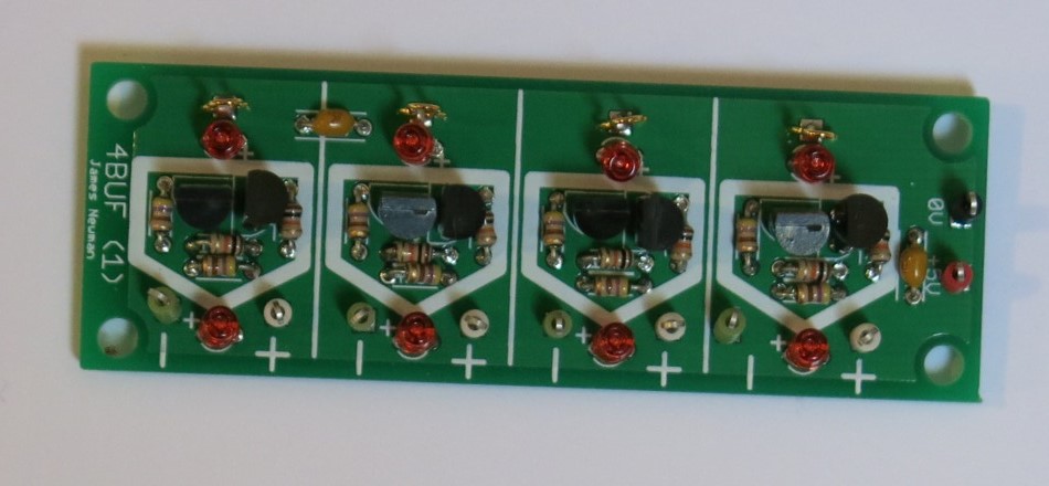
| 4 BUF (design files) |
 |
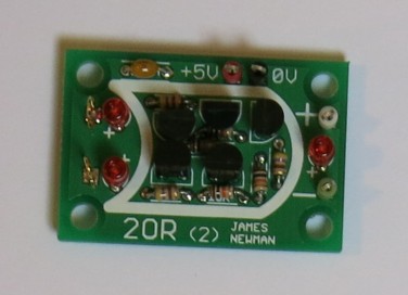
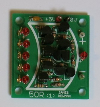
| 5OR (design files) |
 |
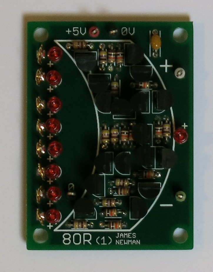
| 8OR (design files) |
 |
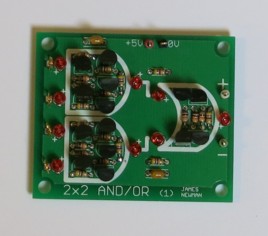
| 2x2AND OR (design files) |
 |
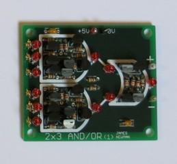
| 2x3AND OR (design files) |
 |
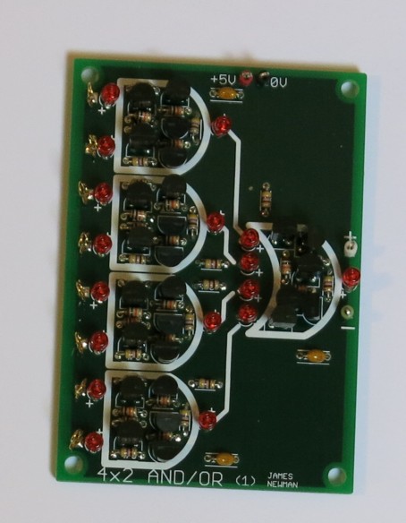
| 4x2AND OR (design files) |
 |
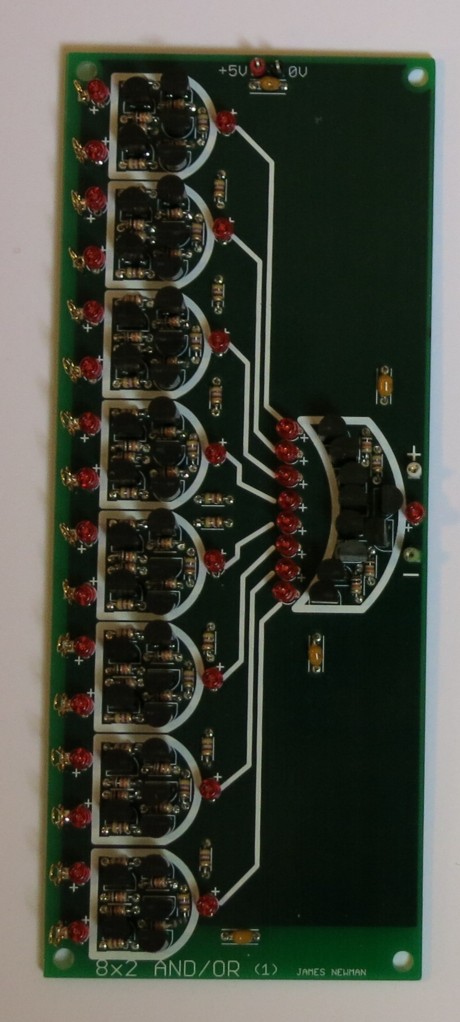
| 8x2AND OR Somehow when doing this board I messed up the power plane so it didn't extend over the whole board. So there's a few wires underneath to sort things out. (design files) |
 |
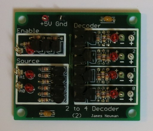
| 2 to 4 DECODE (design files) |
 |
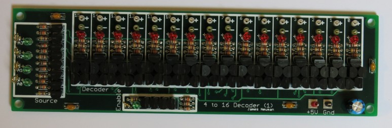
| 4 to 16 DECODE (design files) |
 |
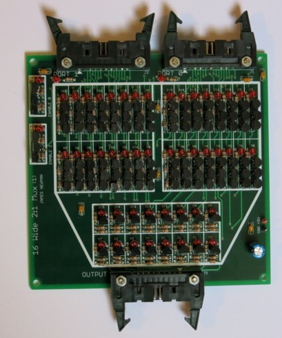
| 16x2MUX (design files) |
 |
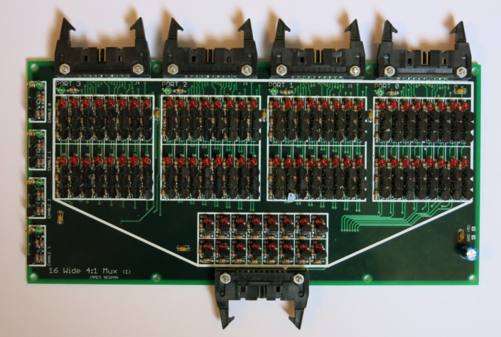
| 16x4MUX This is the most tedious to solder. (design files) |
 |
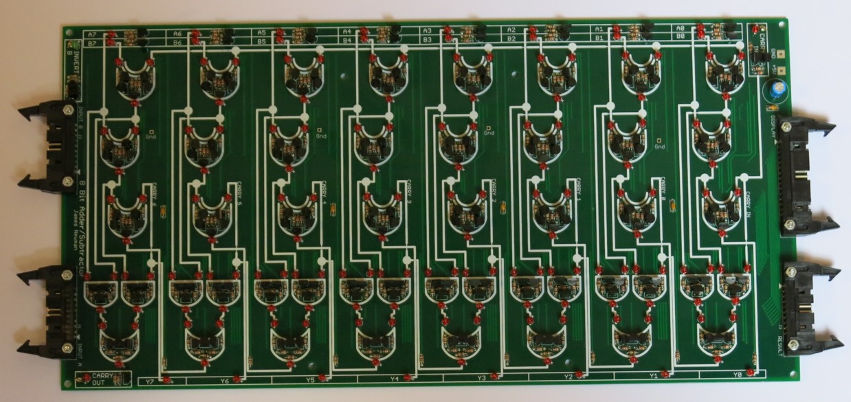
| 8BIT
ADD/SUB This is my favourite board (design files) |
 |
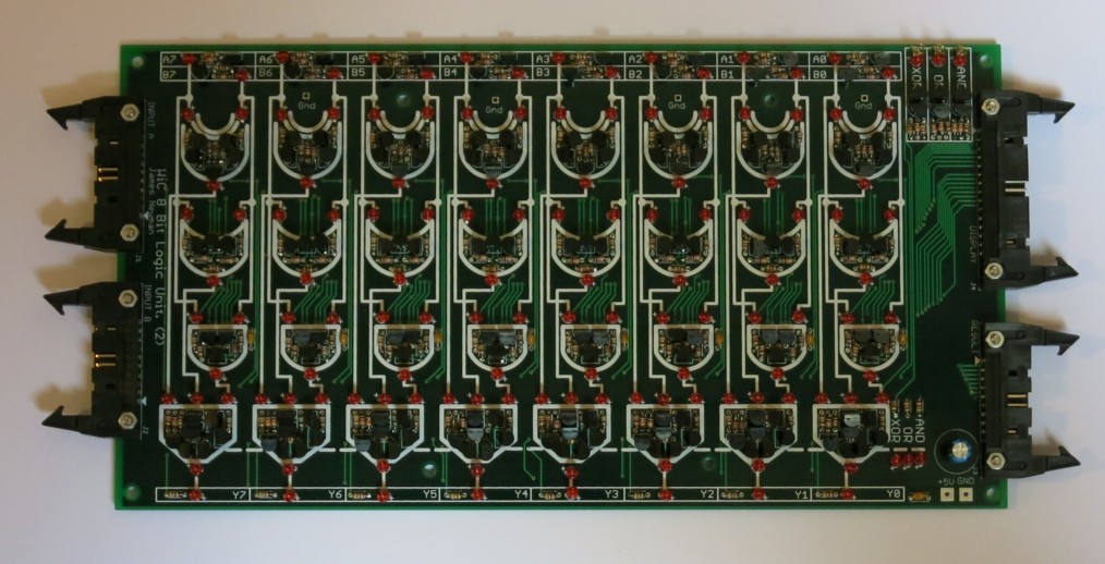
| 8BIT LOGIC (design files) |
 |
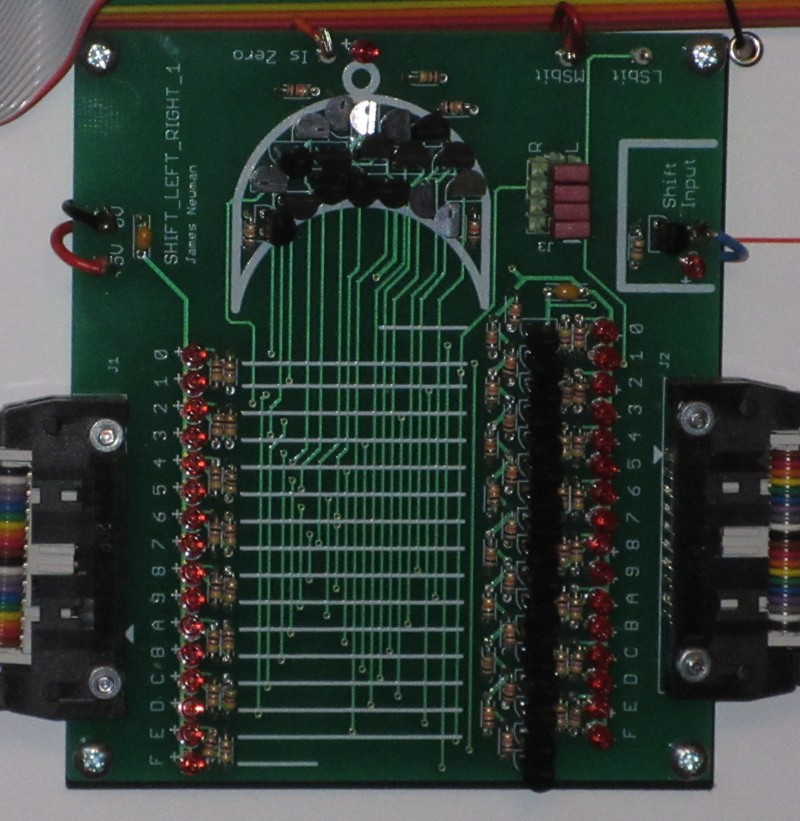
| Shifter The shifting is just by wiring from one connector to the other with an offset. Depending on which side you call the input and which the output its a left or right shifter. It also generates some status data (is zero etc). (design files) |
 |
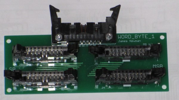
| Word Byte Converter This splits a 16 bus into an LSB and MSB, or vice versa. Its purely wiring. (design files) |
 |
Display
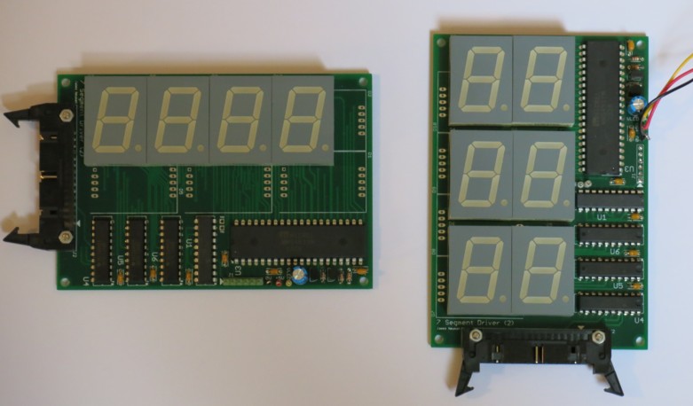
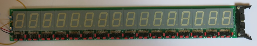
I spent a bit of time trying to work out how to do the 7-segment display using discrete transistors but the answer is vast. Really, really big. It would have near doubled the size of the thing and the circuitry for the display would have obscured the circuitry for the processor which would have undermined what I was trying to do. As its only for debug and not proper function I went for chips. This is definitely NOT cheating, it is just for debug. It is irritating though.| 3x2, 4DIGITS Same board, there's two ways of fitting the display. (design files) |
 |
| STATUS_DISPLAY Used for state machine and status flags, only does 0 & 1, or - & 1. (design files) |
 |
Connectivity
I ended up needing a lot simple boards just to be able to connect things together in a reasonably manner. Some of early decisions were a little poor, this should have been easier.
| Data bus breakout. This is just used for generating constant values. (design files) |
 |
| Data bus breakout with display. (design files) |
 |
| Address bus breakout (design files) |
 |
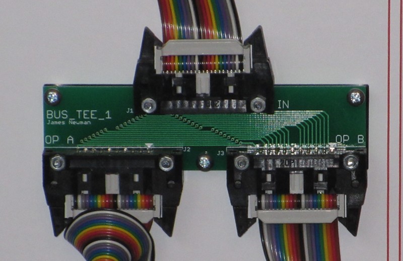
| Data bus Tee This is purely wiring. (design files) |
 |
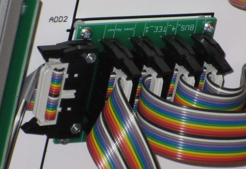
| Data bus Tee (buffered) I use this when I want to tee a bus to send it to a different frame. (design files) |
 |
| Data bus Tee (4 way) (design files) |
 |
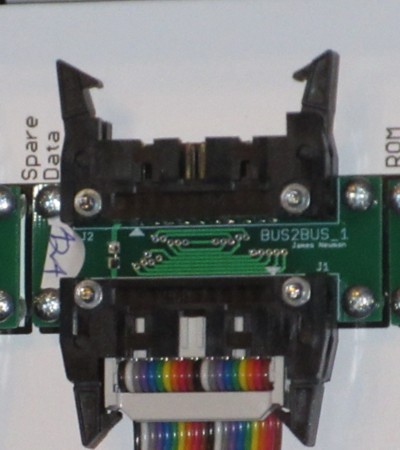
| Data bus to data bus Used on the edge of modules. (design files) |
 |
| frame to frame This combines four data buses together to make a 64 way bus for joining frames together (a small number of wide cables is easier to deal with than lots of small ones). (design files) |
  |
| frame to frame (protected) Does the same as above but I added some protection circuitry for when its used for incoming buses. I don't know if its necessary, or if I did it correctly. (design files) |
 |
| frame to frame memory connection This combines the address and data bus into a single cable for transferring between frames. It includes protection circuitry for inputs. (design files) |
  |
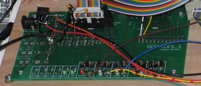
| Services This is a partially populated version that I used for the processor emulator during testing. (design files) |
 |
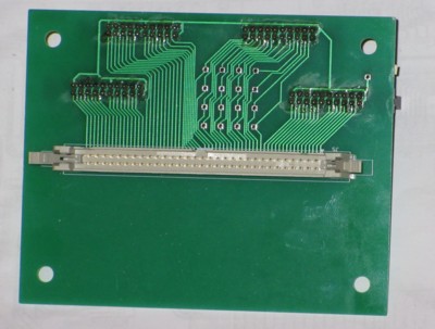
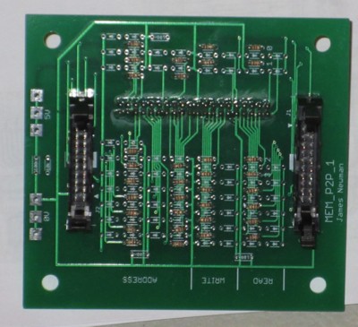
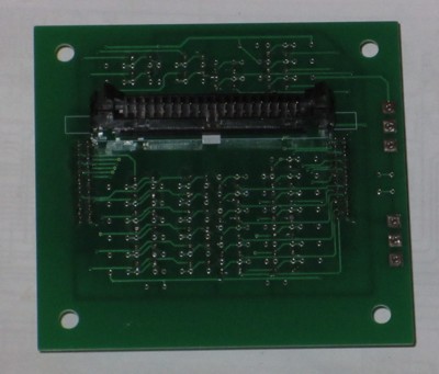
Memory
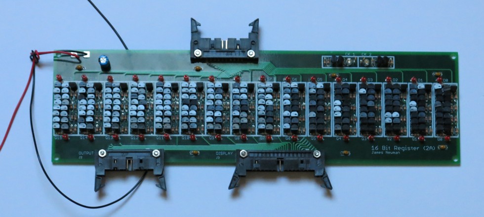
| 16 bit register (design files) |
 |
| RAM (design files) |
 |
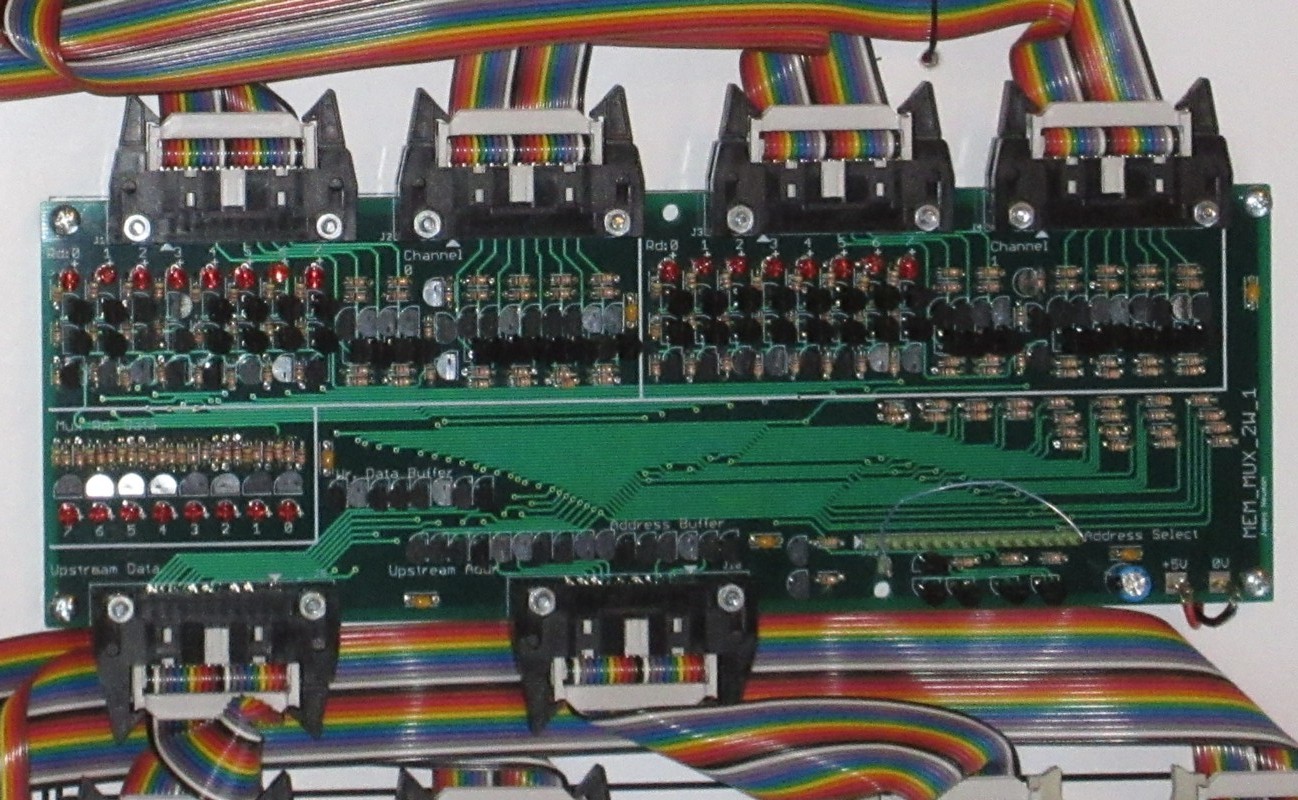
| I/O Mux 4 way (design files) |
 |
| I/O Mux 2 way (design files) |
 |
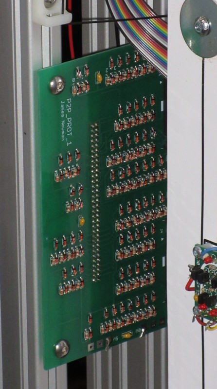
Test
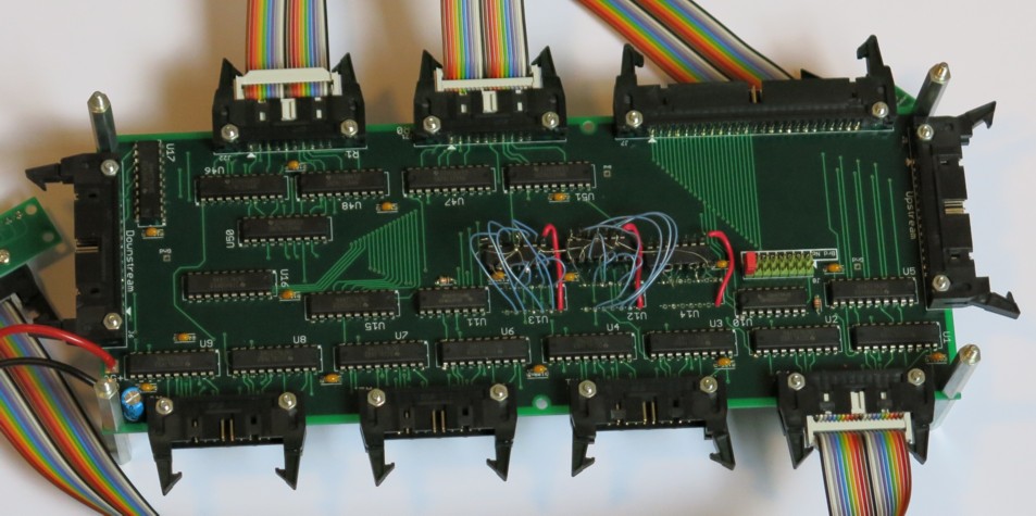
| Test Board To test the larger scale structures I need a huge amount of I/O out of the PC so I built an I/O expander. These can be daisy chained (I hope, not tried it yet) to give me what I need to test the largest modules. Made a stupid stupid mistake on the pinout for the very simplest chip. Hence the carbuncle. (design files) |
 |
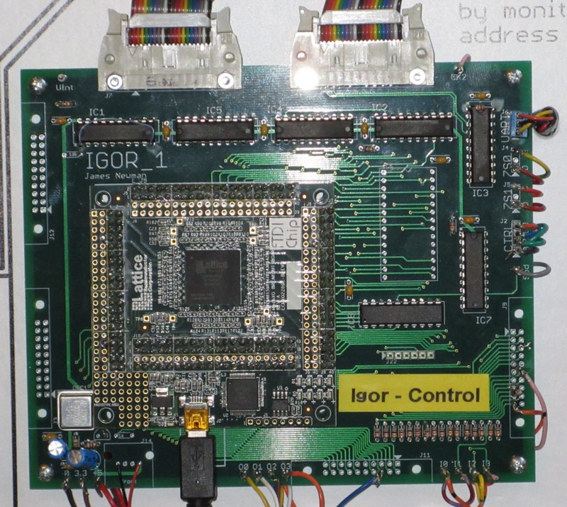
| IGOR This consists of an FPGA development board from Lattice piggybacking on a board that provides 3 to 5V level translation to allow it to talk to the Megaprocessor. I was originally only going to build one of these but I ended up splitting out its functions (control, memory, peripherals) to try and make it easier to see what was happening rather than just having one board doing magic. He's described in more detail here . (design files) |
 |

© 2014-2016 James Newman.