 Architecture
Introduction
The Megaprocessor is a 16 bit processor. There are four general purpose 16 bit registers: R0, R1, R2, R3. There is a program counter, PC. A register dedicated as the stack pointer SP. And a processor status register, PS. For computation there is a 16 bit ALU and a 16 bit adder. The registers and compute resources are connected via multiplexors which allow the Megaprocessor to configure its data flows in different ways for different instructions. For most instructions the processor is configured in this way:
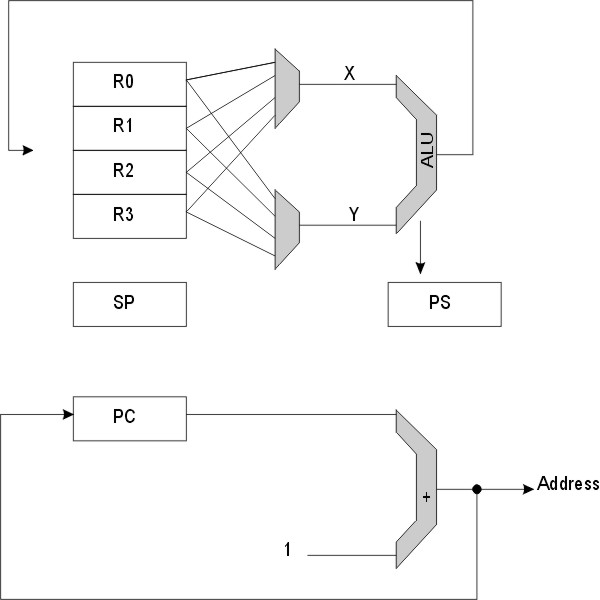
In this configuration the ALU takes two operands from the General Purpose Registers and writes the result of a calculation back to one of them. Concurrently with this the PC is being updated to get the next instruction.
The operation of the Megaprocessor is controlled by a state machine which is described here.
Nearly all instructions cause the PS register to be updated in some way, the meaning of the PS register bits are described here.
All registers are 16 bits wide and all operations are 16 bit orientated (there are no byte operations). The Megaprocessor has a load/store architecture: ALU operations can take place only between the general purpose registers so data must first be loaded into registers before being operated on and the results stored as required.
Whilst all internal data paths are 16 bits wide the external
data bus is 8 bits wide. There is a 64K address space. There is
no mechanism for stalling the processor, all byte accesses take
one cycle. Data can be loaded/stored to memory as either bytes
(8 bits) or words (16 bits). Words are stored in memory in
littleendian format. Bytes loaded from memory are zero extended
to 16 bits to fill a register. There is a SXT (sign extend)
instruction to sign extend the LSB of a register if the byte
should have been interpreted as a signed value.
I've added several peripherals, they're described here.
Instruction Set
Instructions consist of 8 bit opcodes with up to two bytes of following immediate data. This means that there are 256 possible instructions, and all are used. They are divided into 16 groups of 16 as per the table below.
| Group: | MOVER | AND | XOR | OR | ADD | ADDQ | SUB | CMP |
| 0x00 | 0x10 | 0x20 | 0x30 | 0x40 | 0x50 | 0x60 | 0x70 | |
| 0x00 | sxt r0 | test r0 | xor r0,r0 | inv r0 | add r0,r0 | addq r0,#2 | neg r0 | abs r0 |
| 0x01 | move r1,r0 | and r1,r0 | xor r1,r0 | or r1,r0 | add r1,r0 | addq r1,#2 | sub r1,r0 | cmp r1,r0 |
| 0x02 | move r2,r0 | and r2,r0 | xor r2,r0 | or r2,r0 | add r2,r0 | addq r2,#2 | sub r2,r0 | cmp r2,r0 |
| 0x03 | move r3,r0 | and r3,r0 | xor r3,r0 | or r3,r0 | add r3,r0 | addq r3,#2 | sub r3,r0 | cmp r3,r0 |
| 0x04 | move r0,r1 | and r0,r1 | xor r0,r1 | or r0,r1 | add r0,r1 | addq r0,#1 | sub r0,r1 | cmp r0,r1 |
| 0x05 | sxt r1 | test r1 | xor r1,r1 | inv r1 | add r1,r1 | addq r1,#1 | neg r1 | abs r1 |
| 0x06 | move r2,r1 | and r2,r1 | xor r2,r1 | or r2,r1 | add r2,r1 | addq r2,#1 | sub r2,r1 | cmp r2,r1 |
| 0x07 | move r3,r1 | and r3,r1 | xor r3,r1 | or r3,r1 | add r3,r1 | addq r3,#1 | sub r3,r1 | cmp r3,r1 |
| 0x08 | move r0,r2 | and r0,r2 | xor r0,r2 | or r0,r2 | add r0,r2 | addq r0,#-2 | sub r0,r2 | cmp r0,r2 |
| 0x09 | move r1,r2 | and r1,r2 | xor r1,r2 | or r1,r2 | add r1,r2 | addq r1,#-2 | sub r1,r2 | cmp r1,r2 |
| 0x0A | sxt r2 | test r2 | xor r2,r2 | inv r2 | add r2,r2 | addq r2,#-2 | neg r2 | abs r2 |
| 0x0B | move r3,r2 | and r3,r2 | xor r3,r2 | or r3,r2 | add r3,r2 | addq r3,#-2 | sub r3,r2 | cmp r3,r2 |
| 0x0C | move r0,r3 | and r0,r3 | xor r0,r3 | or r0,r3 | add r0,r3 | addq r0,#-1 | sub r0,r3 | cmp r0,r3 |
| 0x0D | move r1,r3 | and r1,r3 | xor r1,r3 | or r1,r3 | add r1,r3 | addq r1,#-1 | sub r1,r3 | cmp r1,r3 |
| 0x0E | move r2,r3 | and r2,r3 | xor r2,r3 | or r2,r3 | add r2,r3 | addq r2,#-1 | sub r2,r3 | cmp r2,r3 |
| 0x0F | sxt r3 | test r3 | xor r3,r3 | inv r3 | add r3,r3 | addq r3,#-1 | neg r3 | abs r3 |
| Group: | Indirect | PostInc | Stack rel | Absolute | Push/Pop | Immediate | Branch | Misc |
| 0x80 | 0x90 | 0xA0 | 0xB0 | 0xC0 | 0xD0 | 0xE0 | 0xF0 | |
| 0x00 | ld.w r0,(r2) | ld.w r0,(r2++) | ld.w r0,(sp+m) | ld.w r0,addr | pop r0 | ld.w r0,#data | buc dd | move r0,sp |
| 0x01 | ld.w r1,(r2) | ld.w r1,(r2++) | ld.w r1,(sp+m) | ld.w r1,addr | pop r1 | ld.w r1,#data | bus dd | move sp,r0 |
| 0x02 | ld.w r0,(r3) | ld.w r0,(r3++) | ld.w r2,(sp+m) | ld.w r2,addr | pop r2 | ld.w r2,#data | bhi dd | jmp (r0) |
| 0x03 | ld.w r1,(r3) | ld.w r1,(r3++) | ld.w r3,(sp+m) | ld.w r3,addr | pop r3 | ld.w r3#data | bls dd | jmp addr |
| 0x04 | ld.b r0,(r2) | ld.b r0,(r2++) | ld.b r0,(sp+m) | ld.b r0,addr | pop ps | ld.b r0,#data | bcc dd | andi ps,#data |
| 0x05 | ld.b r1,(r2) | ld.b r1,(r2++) | ld.b r1,(sp+m) | ld.b r1,addr | [NOP2] | ld.b r1,#data | bcs dd | ori ps,#data |
| 0x06 | ld.b r0,(r3) | ld.b r0,(r3++) | ld.b r2,(sp+m) | ld.b r2,addr | ret | ld.b r2,#data | bne dd | add.b sp,#data |
| 0x07 | ld.b r1,(r3) | ld.b r1,(r3++) | ld.b r3,(sp+m) | ld.b r3,addr | reti | ld.b r3#data | beq dd | sqrt |
| 0x08 | st.w (r2),r0 | st.w (r2++),r0 | st.w (sp+m),r0 | st.w addr,r0 | push r0 | shift r0,descr | bvc dd | mulu |
| 0x09 | st.w (r2),r1 | st.w (r2++),r1 | st.w (sp+m),r1 | st.w addr,r1 | push r1 | shift r1,descr | bvs dd | muls |
| 0x0A | st.w (r3),r0 | st.w (r3++),r0 | st.w (sp+m),r2 | st.w addr,r2 | push r2 | shift r2,descr | bpl dd | divu |
| 0x0B | st.w (r3),r1 | st.w (r3++),r1 | st.w (sp+m),r3 | st.w addr,r3 | push r3 | shift r3,descr | bmi dd | divs |
| 0x0C | st.b (r2),r0 | st.b (r2++),r0 | st.b (sp+m),r0 | st.b addr,r0 | push ps | bit r0,descr | bge dd | addx r0,r1 |
| 0x0D | st.b (r2),r1 | st.b (r2++),r1 | st.b (sp+m),r1 | st.b addr,r1 | trap #n | bit r1,descr | blt dd | subx r0,r1 |
| 0x0E | st.b (r3),r0 | st.b (r3++),r0 | st.b (sp+m),r2 | st.b addr,r2 | jsr (r0) | bit r2,descr | bgt dd | negx r0 |
| 0x0F | st.b (r3),r1 | st.b (r3++),r1 | st.b (sp+m),r3 | st.b addr,r3 | jsr addr | bit r3,descr | ble dd | nop |
A detailed description of each instruction is in this document.
There is one stage of pipelining, the next instruction is fetched whilst processing the current instruction. This means that in general instructions take one cycle per byte of memory access required (including the instruction itself). e.g. simple ALU instruction are one byte long, and take one cycle to execute. Loading a word from an absolute address takes 5 cycles as 5 bytes of memory access are required: 1 for the instruction, 2 for the address, 2 to load the word.
The multiply, divide and square root instructions are implemented using iterative algorithms described here.To implement some of the more complex instructions there is a "helper/hidden" register, H, which is used by the processor as a scratchpad. The H register does not carry any information from one instruction to the next.
Opcode 0xC5 is no longer used and is currently mapped to NOP.
Exceptions
There are four exceptions. For each exception there is an associated vector to which the processor will jump after completing exception processing. The base address for the vectors may be 0x0000 or 0xFFF0 selected by hardware switch. The vectors are offsets of 0x0, 0x4, 0x8 and 0xC relative to the vector base.
Structure
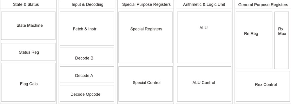
The Megaprocessor was designed as a set of 10 subsystems
- State machine
- Status register
- Instruction Fetch
- Instruction Decoding
- Program Counter (PC)
- Stack Pointer (SP)
- Helper Register (H)
- Address & Write data
- ALU
- General Purpose Registers (R0..R3)
For construction these were mapped onto 14 modules mounted in 5 frames as shown below:

© 2014-2016 James Newman.