 History & Evolution
I didn't plan on ending up here. I started by wanting to learn about transistors. Things got out of hand.
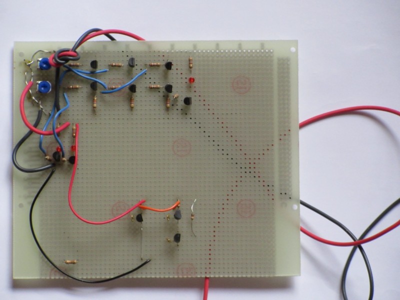
The project started a few years back when I decided I wanted to learn about transistors. My work at the time was a mix of software and FPGAs for various radio communication systems. As part of this I got involved in conversations with the folk doing the analogue electronics design and wanted to better understand what they were up to. It took me a while to get round to but eventually somewhen around 2011/2012 I bought myself a few components and wired up a little test circuit with a transistor and a couple of variable resistors so I could twiddle things and see what happened. The board below is the one I used for my early experiments, the original circuit is probably long gone but the pots are still there on top left.
The first circuit was not much fun, not very interesting, didn't hold my attention for more than a couple of minutes. I quickly decided that the only way to learn about transistors was to build something. But what ? I couldn't think of anything so I put the board to one side and did something else.
Inspiration came a few months later. A potential project came in for a telemetry system that would have to operate in a hostile environment (just behind the drill bit of an oil well). Hot. Very hot. My colleagues and I cast around trying to find components, and in particular processors, that could operate under the required conditions. Initially we couldn't find processors, but we could find some discrete logic devices that could handle the heat. It seemed to me that the required system was sufficiently simple that it was quite feasible to build it from discrete logic. I recall being gently mocked for the suggestion. I can't remember quite how the conversation went after that but at some point I made the throwaway remark that when it came to debugging discrete logic then at least we'd be able to see everything that was happening in the logic. We could even put LEDs on all the signals and watch it operate. Which would be fun. But then we did manage to find some high temperature processors and shortly afterwards the project went away anyway,. Which rather ended the discussion. Or at least it should have. But it had got me thinking about what it would be like to see logic working with LEDs. And then I remembered my abandoned transistor. So I decided that the first thing I should build was a logic gate, and I should put an LED on it. I think that's on the board above as well.
Having built the circuit it struck me that not only could you see the logic state with the LED, you could also layout the board to see all of the transistors and how they were connected together. And then I tried to imagine what it would be like to see an entire processor with all of its transistors laid out for you to see, and with all the logic levels visible so you could watch it work. You would actually SEE the logic. And not just that. It would likely be fairly large so you would want to make it in a sort of wraparound way so you could see everything at the same time. Which would mean that you would be actually sitting inside a processor. How cool would that be!
So how would you do it ? At that time I don't think I had any intention of actually building such a thing. It was more an interesting thought experiment... how would you do it?
I messed around with a few ideas looking at various aspects of a processor wondering what might be doable and then thought why not actually build something. Best way to learn, which afterall is what the original point of the exercise was. So I did. Initially I tried to do it by wiring components together on prototype boards but that was pretty tedious and I spent more time sorting out my wiring than anything else. So I thought why not try doing a PCB. And here it is:
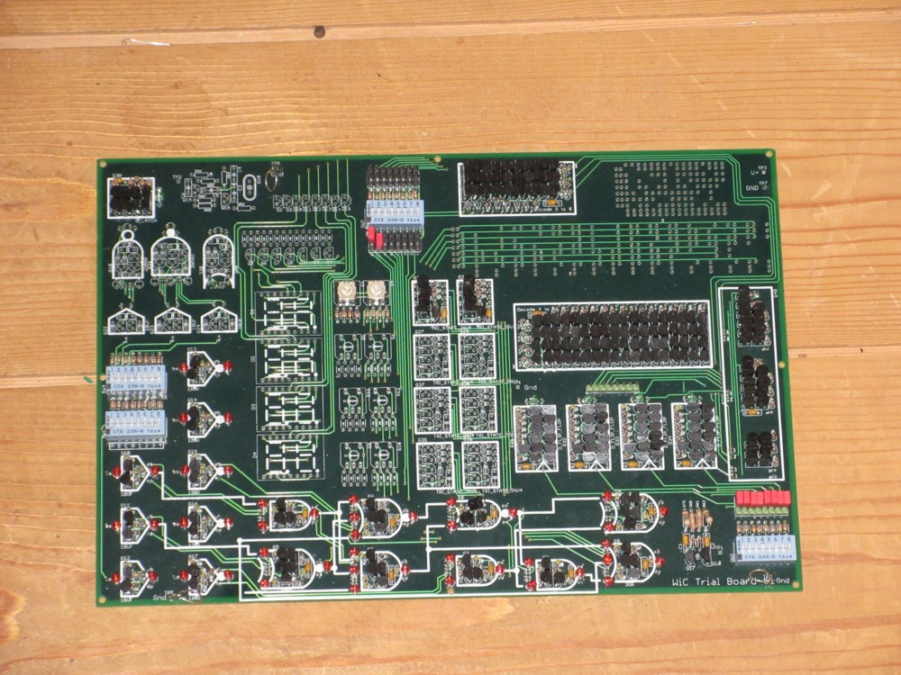
It was a collection of fragmentary ideas so that I could try things out, but at least starting with things correctly wired together. You might be able to see its called "WiC Trial Board". I was originally calling the project my "Walk in Computer". The name changed to Megaprocessor sometime in 2014. I learnt quite a lot from this board.
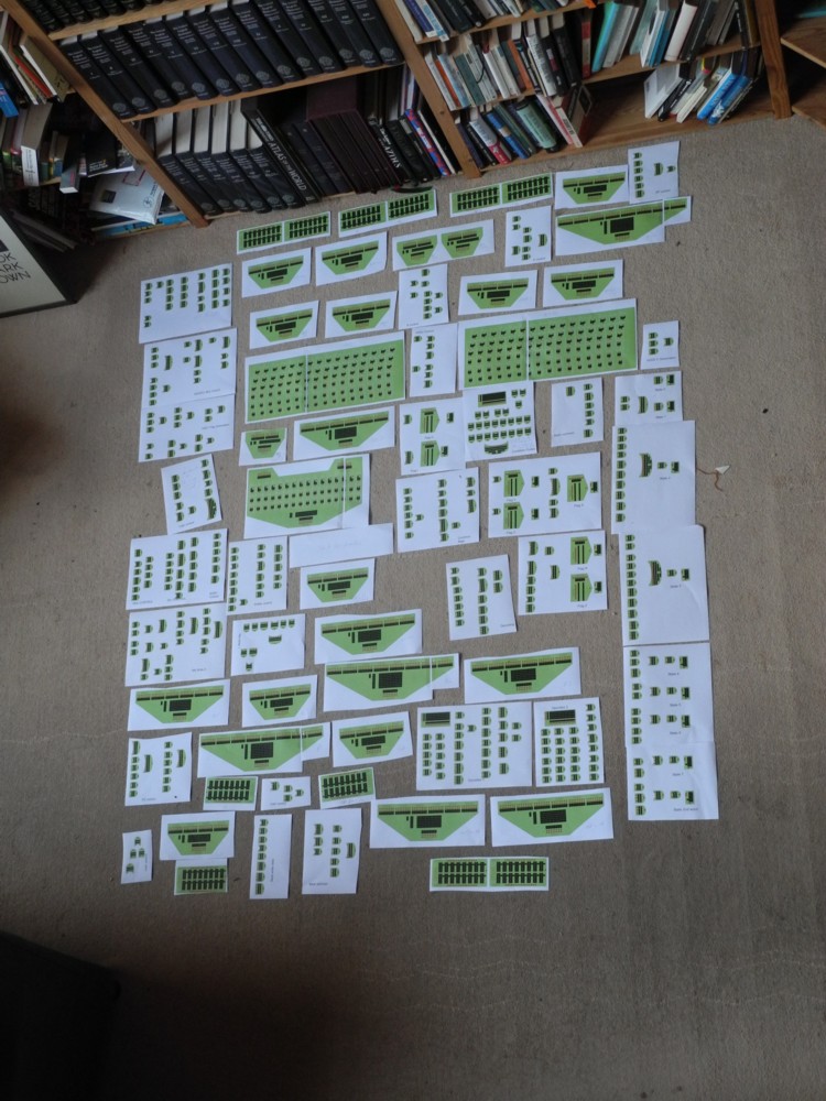
Whilst absorbing the lessons from the trial board I turned my attention to the logic design for the processor itself. What should it do, how would it do it. I spent many happy hours trying out different architectures and choices of instruction sets. Eventually I had a reasonably stable idea as to what would be big enough to plausibly claim to be a proper processor (I could see no merit at all in building the simplest possible processor) yet small enough to be feasible. So I coded up a model in software to try and get a feel for how big it would be. It didn't look to scary. So I tried to work out how large each of the logic gates would be, printed out pictures and built myself a paper processor. This was mid 2013.
It was about 2m a side. Now that to me seemed an entirely sensible size. To be sure not big enough to walk in but actually that meant it was small enough to be practicable as maybe a piece of wall art. Perhaps not to everyones taste, but I could see it taking up a wall in my study. A fair challenge but feasible. Should be fun. Lets do it.
(I think my guess at the time was for the project taking maybe a year or so of a few evenings a week, costing maybe a few thousand. Hah!)
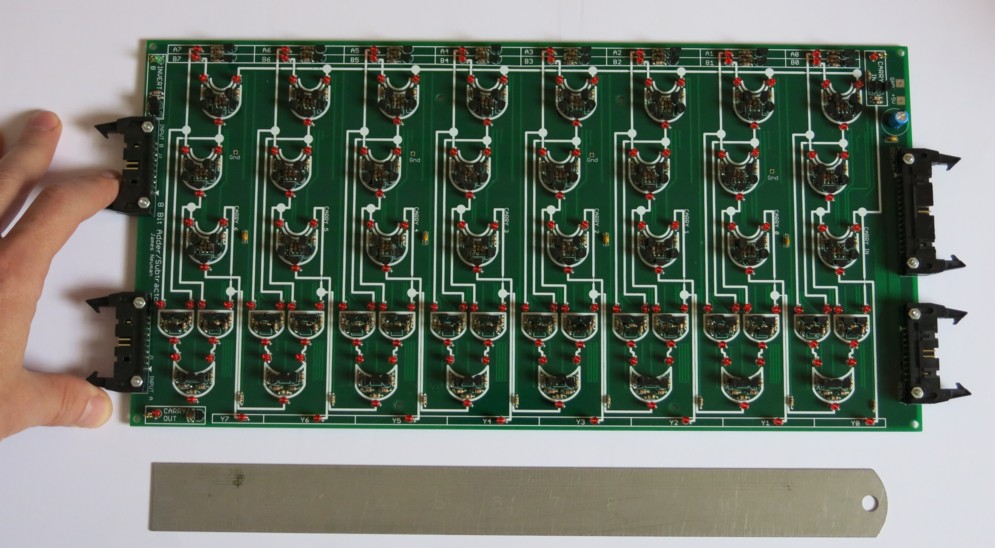
On the electronics side things progressed reasonably well. This was doing the various boards I need. The 8 bit adder/subtractor arrived April 2014. It's is my favourite board.
On the logic design side progress was not so straightforward. A couple of things happened. Firstly I became a bit more ambitious. It's my processor, it should do multiply and divide. I was interested in how these operations could be done, and the point of this project was still to learn stuff so I thought I should implement them. This added a bit of complexity. The second thing that happened was more subtle but much more costly. The starting point for this adventure had been the idea of actually being able to see logic work. But the more I contemplated my initial paper layout the more uneasy I felt about this. To be sure you'd be able to see the logic levels, but would their operation make sense. Would it be possible to see how things were connected and why what happened was happening? So I started restructuring the layout to group together related logic in a much more explicit manner. This is when the size really started to bloat; to show the relationships between elements you had to have some space.
In Sep 2014 I had another go at trying to work out what the processor might look like. And now I really should have noticed the warning signs. I had to do it quarter scale to fit on my living room floor.
It was 3m long and about 30 cm tall quarter scale. So full size 12×1 m. Hmmm. This is where I should have stopped. I live in a bungalow. Its not huge. But it is quite long. In fact the hallway is about 12m long and I could just picture having the processor mounted along one wall. Bit like the Bayeux tapestry. (But even better). So nearly there, I thought, lets just go a bit further and see if this would work.
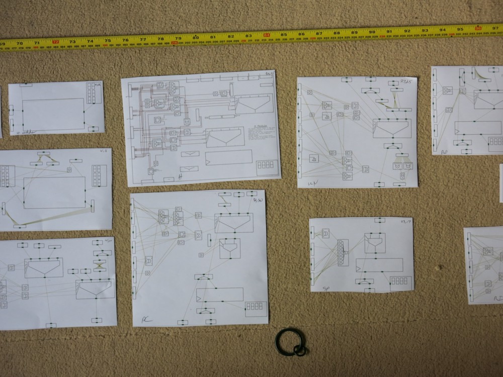
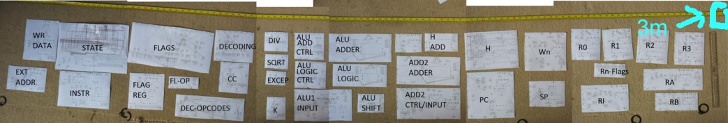
End of 2014/early in 2015 the realisation began to dawn on me that there was a dreadful horror buried in my new layout. Connectivity. I'd split the processor into nearly 40 modules. Each of the modules had a nice clearly defined purpose, and showed how the control logic caused the operation of the module. But this led to an insane number of connections as signals had to be routed to multiple modules. After a bit I decided that this wasn't really buildable. So I threw away that layout and started again trying to group things together not just by common function, but also by common signals. This led to the current structure of 14 modules mounted in 5 frames. It's still about 12m long, but is now 2m tall. (This is going to be a problem for my house).
By Sep 2014 I was sufficiently confident to begin construction and completed the first module in Jan 2015. The soldering and construction finished about Jan 2016. At time of writing (April 2015) we're in the integration (and documentation) phase.
- Home
- Vital Statistics
- Progress
- Architecture
- Stepping Stones
- Programming
- Peripherals
- Construction
- Cost & Materials
- Good, Bad & Ugly
- History
- Build Faults
- Flip Flops
- Modelling
- Architecture Choice
- Logic Type
- 7 segment
- Board Shape
- Dual Output
- ALU
- SRAM
- Speed
- Speed 2
- Buses
- Area
- Efficiency
- LED supply
- Multiplexor Problem
- Multiplexor Errors
- Surface Mount
- Solder
- Health & Safety
- Web
- Links
- Contact

© 2014-2016 James Newman.