 SRAM
SRAM
I use an average of just over 11 transistors per RAM bit. Wikipedia (and most other sources) say the normal answer is 6 with 4 being possible.
When looking at the various diagrams of 6T cells I wasn't confident I fully understood what I was seeing.

What type exactly are the transistors being shown. And is everything shown ? any resistors/capacitors not shown for clarity ? And whilst it might work on a chip, will it work with discretes ? Lacking confidence I went for a cell built around a set-reset latch. One of my bits looks like:
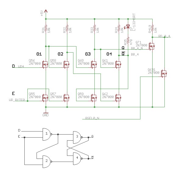
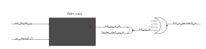
The bits of each byte are mutiplexed with OR gates (this was shortly after I was traumatised by my multiplexor problem and so was overly cautious):
So 4 transistors to make the memory itself with 2 cross coupled NAND gates (G3 + G4), and then two transisitors for each NAND gate for generating the set and reset signals (G1 + G2). Which makes 8.
I then use 2 transistors for an output stage . Which makes 10.
And then there's another transistor (not shown) being used for the byte multiplexor. Which makes 11.
There's a bunch of other transistors being used for address decoding etc which brings the average up to 11 and a bit.
In the privacy of my mind I compared the 11 not with the 6 that the rest of the world gets but with 9 as in 6 + 3. I assumed that most if not all of the 3 transistors I use to stitch the cell to the rest of the memory will be needed anyway. I was probably being generous to myself . Anyway I decided to run with this design as I was reasonably sure it would, or could be made to, work. As it happens my first version did work perfectly well as a memory. Unfortunately it also worked quite well as an inverter, everything was remembered but came out upside down.
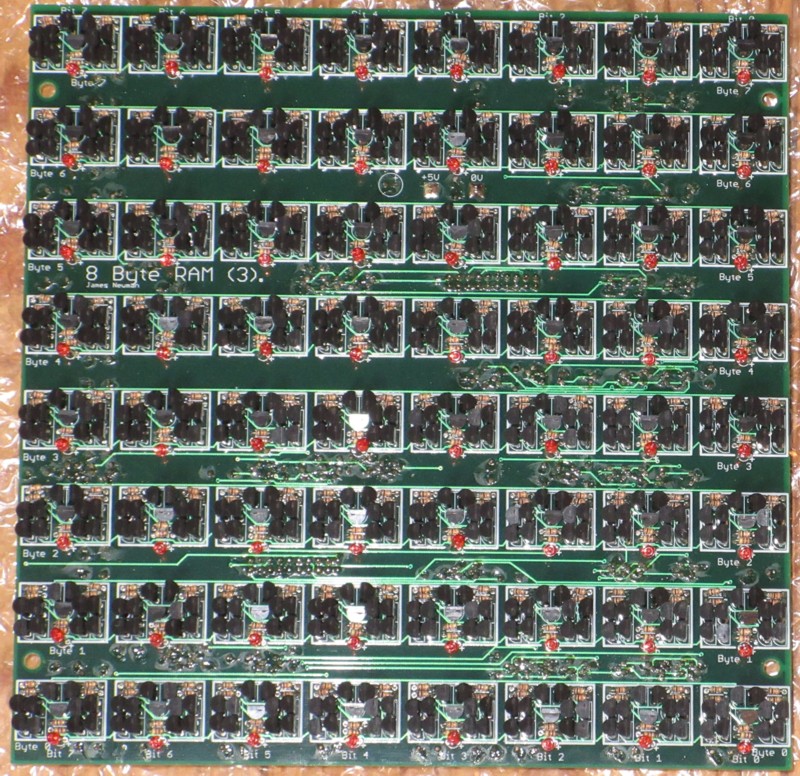
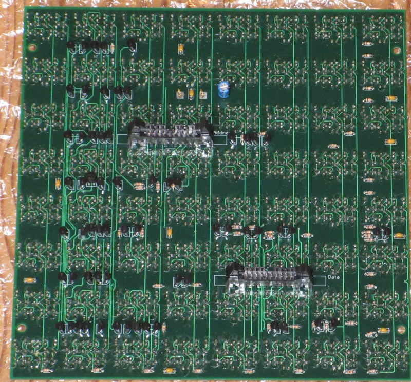
One feature of the board design I put a bit of effort into was to make sure it would tessellate well. Whilst being able to see the memory contents was the initial reason for building it from discrete I also realised that it could act as a display. So each bit is aligned on a square grid and the boards fit together to extend this grid. To do that I had to put some components on the back of the board.
[Note: when gathering data for this page I had another look for others trying this and found Instructables and Mostafa Abd El-Aziz. They do better than I did. But I take comfort from the fact that my suspicion about the transistors was borne out by their experience. At the time I was designing my memory I'd have really struggled to understand and solve the issues caused by non-ideal transistors. Both authors ended up making an 8T cell with two transistors being replaced by pairs to workaround the non-ideality of the devices..]
If I'd known just how long it would take to build the memory I'd have tried a lot lot harder to make it smaller.
A couple of people have asked if I considered building DRAM. I did have a little look around at the start to see if anyone had done it before and I did find someone but unfortunately I've lost the link and can't remember much about it. The main reason I didn't pursue it with much vigour is the problem of refresh. With modern electronics a refresh controller is fairly straightforward, but building one out of discretes would be quite hard work. A couple of counters and some extra multiplexors, not much less than the Megaprocessors ALU itself. Rather than having a separate refresh controller you could have the processor do the refresh by having it run through the memory every now and then using, say, a timer interrupt. But a key feature of the Megaprocessor is that you can run it very very slowly indeed (to watch the logic) and then you'd almost certainly not refresh quickly enough.
Mark B. wrote to suggest I could have used multi-colour LEDs. The same red/off for a 1/0 but changing colour when the cell was accessed and/or being written to. Quite an interesting idea.
- Home
- Vital Statistics
- Progress
- Architecture
- Stepping Stones
- Programming
- Peripherals
- Construction
- Cost & Materials
- Good, Bad & Ugly
- History
- Build Faults
- Flip Flops
- Modelling
- Architecture Choice
- Logic Type
- 7 segment
- Board Shape
- Dual Output
- ALU
- SRAM
- Speed
- Speed 2
- Buses
- Area
- Efficiency
- LED supply
- Multiplexor Problem
- Multiplexor Errors
- Surface Mount
- Solder
- Health & Safety
- Web
- Links
- Contact

© 2014-2016 James Newman.